OUTLINE:
Methods for Copying Double-Sided PCB and Multi-Layer Boards PCB
 204
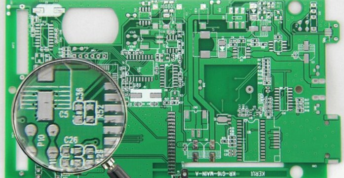
204PCB copying is a complex process that involves replicating the layout and design of an existing circuit board. The differences in copying methods between double-sided and multi-layer PCBs are significant, and understanding these variances is crucial for successful replication. In this article, we will explore the steps involved in each method and highlight the key distinctions.

When it comes to double-sided PCB copying, the process begins with scanning the upper and lower layers of the circuit board to be replicated. This scanning process captures the precise component positions and traces on the board. The scanned images are then imported into PCB design software, such as Quickpcb2005.
In the software, the design engineer recreates the board layout by manually drawing the traces, pads, and components based on the scanned images. The goal is to replicate the original layout as accurately as possible. Once the layout is complete, it is saved as a B2P file, which contains all the necessary data for the double-sided PCB.
To ensure accuracy, the engineer repeats the process for the opposite layer of the PCB. The second scanned image is imported into the software, and the layout is recreated by drawing the traces, pads, and components. The engineer then merges the top and bottom layer data into a single B2P file, representing the complete double-sided PCB.
After the B2P file is prepared, it can be exported as a PCB file. This file can be further modified if necessary or sent directly to a PCB manufacturing facility for production. The manufacturing facility will use the PCB file to fabricate the replicated double-sided PCB, which can then be populated with the required components. Finally, the replicated board undergoes testing to ensure its electronic performance matches that of the original board.
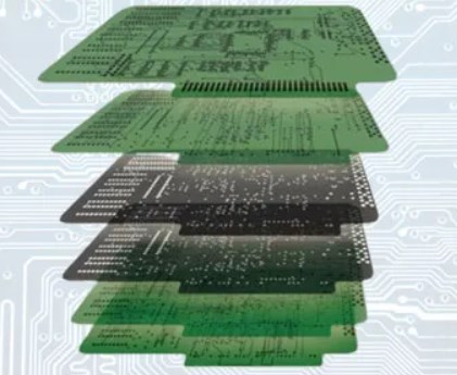
In contrast, multi-layer PCB copying is a more intricate process due to the presence of internal layers that are not visible from the outside. Replicating a multi-layer board typically involves using multiple double-sided boards to recreate the internal layers. The initial steps of scanning and recreating the top and bottom layers are the same as in the double-sided method.

However, to access the internal layers, a technique called sanding is employed. Sandpaper is used to gradually remove the outer layers of the replicated boards, exposing one internal layer at a time. This process requires careful precision to avoid damaging the board or losing data. Once an internal layer is exposed, the engineer cleanses the copper wires and skin to remove any residue.
The sanding and cleansing process is repeated until all desired internal layers are accessible. Each exposed layer is then scanned and recreated using the double-sided PCB copying method mentioned earlier. The recreated layer data is merged with the previously scanned top and bottom layers, resulting in a complete multi-layer PCB layout.
The final step involves exporting the merged layer data as a PCB file, which can be modified, printed, or sent for manufacturing. It is important to note that the replication of multi-layer boards requires meticulous attention to detail and precision, as improper alignment or damage to internal vias and non-conductive holes can lead to issues.
In conclusion, the copying methods for double-sided and multi-layer PCBs differ significantly. Double-sided PCB copying involves scanning the top and bottom layers, recreating the layout, and merging the layer data into a complete PCB file. Multi-layer PCB copying requires additional steps, such as sanding the outer layers to access the internal layers and meticulous recreation of each layer. Understanding these differences is vital for successfully replicating PCB designs and ensuring the desired electronic performance of the copied boards.

Disclaimer: The views and opinions expressed by individual authors or forum participants on this website do not represent the views and opinions of Chipsmall, nor do they represent Chipsmall's official policy.

share this blog to:

