OUTLINE:
For Beginners: What is a MOSFET?
 86
86If you're even remotely interested in electronics, you've likely encountered the enigmatic term "MOSFET." But what exactly is it? This guide aims to demystify the MOSFET, delving into its structure, applications, and selection process.

What is a MOSFET
Imagine a microscopic switch controlled not by physical contact, but by a magic wand. That's essentially what a MOSFET is. It's a semiconductor device that regulates the flow of electricity using an electric field generated by a voltage applied to its "gate."
MOSFET, formally known as Metal-Oxide-Semiconductor Field-Effect Transistors, are the tiny workhorses powering the electronic world around us, from your smartphone to your laptop and beyond.
This voltage alters the conductivity of a channel between two terminals called the "source" and the "drain," ultimately controlling the current flow. Think of it as a voltage-controlled faucet for electrons!
Structures of MOSFET
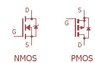
There are two main types of MOSFET: NMOS (N-channel) and PMOS (P-channel). NMOS has a channel made of N-type semiconductors (excess electrons), while PMOS has a channel made of P-type semiconductors (electron deficiency). These channels are further insulated by a layer of silicon dioxide, forming the "metal-oxide-semiconductor" part of the name. Understanding the type and structure is crucial for selecting the right MOSFET for your application.

Applications of MOSFET
The versatility of MOSFET is their true marvel. They're found in practically every electronic device imaginable, including:
Amplifiers: Boosting weak signals, like your radio antenna signal.
Switches: Turning circuits on and off, forming the backbone of digital logic.
Memory circuits: Storing data in computers and other devices.
Power electronics: Controlling high-voltage and high-current applications.
Analog circuits: Performing various signal processing tasks like filtering and conversion.
This is just a glimpse into the vast world of MOS applications!

Advantages VS Disadvantages
Benefits:
High input impedance: Requires minimal current to operate the gate, reducing power consumption in the control circuit.
Low power consumption: Efficient operation, especially in low-current applications, making them ideal for battery-powered devices.
Scalability: Can be miniaturized to very small sizes, enabling integration in complex integrated circuits with high transistor density.
Fast switching speeds: Capable of handling high-frequency signals, making them suitable for applications like radio frequency (RF) amplifiers and switching circuits.
Weakness:
Susceptible to electrostatic discharge (ESD): Sensitive to sudden voltage spikes that can damage the device. Proper handling and circuit design techniques are crucial.
Non-linear behavior: Exhibit non-linear characteristics in certain operating regions, requiring careful design considerations to ensure predictable performance in analog applications.
Higher complexity compared to bipolar junction transistors (BJTs): May require more complex biasing and circuit design techniques compared to BJTs, especially for beginners.
3 Points for Choosing the Right MOSFET
Voltage and Current Ratings
Drain-to-Source Voltage (Vds): This is the maximum voltage the tube can withstand between its drain and source terminals. Choose a tube with a Vds exceeding your expected operating voltage to ensure safety and prevent breakdown.
Gate-to-Source Voltage (Vgs): This is the voltage applied to the gate to turn the channel on. Most NMOSFET require positive Vgs, while PMOS require negative. Select a tube with a Vgs threshold suitable for your control circuitry.
Drain Current (ID): This is the maximum current the tube can handle continuously without overheating. Choose a tube with an ID exceeding your expected operating current to avoid damage and maintain efficiency.
Switching Speed
Rise Time (tr): This is the time it takes for the drain current to rise from 10% to 90% of its maximum value when the gate voltage turns on. Faster switching is desirable for high-frequency applications.
Fall Time (tf): This is the time it takes for the drain current to fall from 90% to 10% of its maximum value when the gate voltage turns off. Faster fall times are crucial for minimizing switching losses.
Package Type
Surface Mount (SMT): Compact and ideal for high-density circuit boards, requiring specialized soldering techniques.
Through-Hole (TH): Easier to solder and handle, but occupy more space on the board.
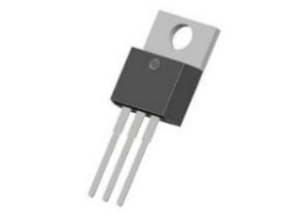
TO-package: Rugged and suitable for high-power applications, often with heat sinks attached.
Conclusion
The MOSFET may seem like a complex beast at first, but understanding its basics unlocks a door to the fascinating world of electronics. From humble beginnings as tiny switches to complex building blocks of modern technology, these "magic wands" of the electronic world deserve our appreciation and understanding. Whether you're a hobbyist tinkering with circuits or an engineer designing the next generation of gadgets, knowledge about MOSFET is an essential tool in your electronic toolbox.

Disclaimer: The views and opinions expressed by individual authors or forum participants on this website do not represent the views and opinions of Chipsmall, nor do they represent Chipsmall's official policy.

share this blog to:

