OUTLINE:
Understanding PCB Bursting and How to Prevent It
 801
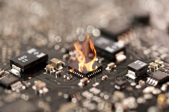
801A Printed Circuit Board (PCB) is an essential component of almost every electronic device we use today. PCB production requires a complex process involving multiple stages, including copper clad plate processing, lamination, etching, drilling, and more. During the copper clad plate processing stage, a phenomenon known as a PCB burst or explosion can occur, causing issues such as copper foil foaming, detachment of the circuit, foaming of the substrate, and delamination.

The root cause of PCB explosions is often due to insufficient heat resistance of the substrate or some problems in the production process. For instance, high operating temperature or long heating time can cause heat stress on the board, leading to bursting. This can happen during thermal shock processes such as dip soldering, wave soldering, or reflow soldering.
One of the main reasons for copper clad bursting is insufficient substrate curing. When the substrate is not cured properly, the heat resistance of the substrate is lowered, making it more prone to bursting during PCB processing or thermal shock. Substrate moisture absorption is another cause of bursting. If the substrate is not stored correctly, it can absorb moisture, and releasing this moisture during PCB processing can cause an explosion. To avoid this, PCB factories should repackage uncoated copper-clad laminates to reduce moisture absorption.
Another reason for PCB bursting is due to low Tg of the substrate. When a copper-clad board with a relatively low Tg is used to produce a circuit board with high heat resistance, the board is more likely to experience issues because of the low heat resistance of the substrate. This can cause the Tg of the substrate to decrease, making it more prone to bursting. Using copper plates with a higher Tg can help address this problem.
Ink used for marking material can also cause PCB bursting. If the ink mark is relatively thick and placed on the surface in contact with the copper foil, it can lower the adhesion of the copper foil, causing the board to burst. To avoid this, manufacturers should consider using thinner ink or placing the ink marks on the opposite side of the copper foil.
To solve the problem of bursting, it is necessary to ensure proper curing of the substrate, control substrate moisture absorption, and use copper plates with a higher Tg. Additionally, using thinner ink for marking material can help prevent PCB bursting. Strict quality control practices can help ensure a qualified PCB board.


Disclaimer: The views and opinions expressed by individual authors or forum participants on this website do not represent the views and opinions of Chipsmall, nor do they represent Chipsmall's official policy.

share this blog to:

