OUTLINE:
An Overview for PCB Designs File Types [Knowledge Base]
 138
138What file type is used for PCB designs? Have you ever thought about how PCB design goes from an idea to a tangible board? What documents do engineers and manufacturers rely on to ensure that circuits can work properly and be produced accurately and without errors?

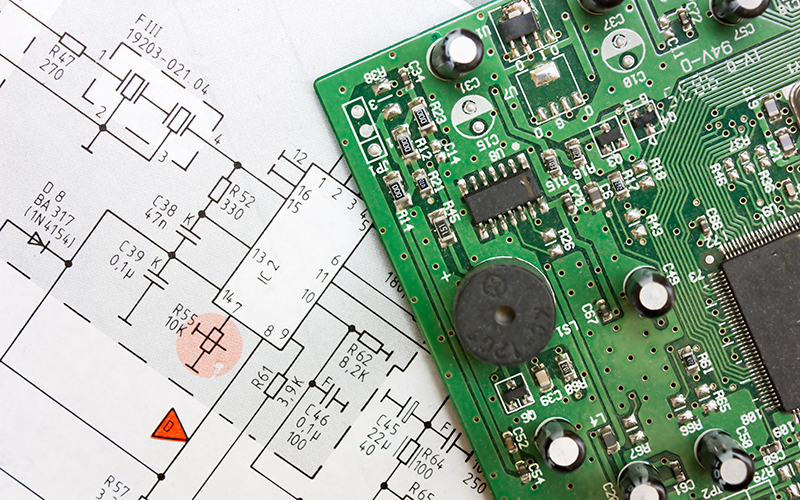
Image Source:Student Circuit
In the world of PCB design, understanding which file types are super important. It can help us make the design process smoother, reduce errors, and ensure smooth communication between the design and manufacturing teams. Come on, let's take a look at which file types play a crucial role in turning PCB design into reality.
How to Define A PCB Design [Basic Knowledge]
PCB, It's that printed circuit board. Designing it is actually designing the appearance and structure of a board, so that electronic components can be stably placed on it and connected to each other. You need to first think about how big and what shape this board should be, then arrange the resistors, capacitors, integrated circuits and other components neatly, and connect them together with wires, just like drawing a picture.
Designing PCBs requires specialized software, which we call CAD tools. These software are very powerful, they can help you draw circuit diagrams, arrange the position of components, and generate some design files, such as Gerber files. These files are like blueprints, ensuring that your design specifications, such as the number of layers on the board, the location of the holes to be drilled, and how to route the circuit, all meet the requirements and standards.
Simply put, PCB design is the process of transforming an idea of a circuit into a real board that can be manufactured and integrated into electronic devices.
What Are the common File Types Used in PCB Designs

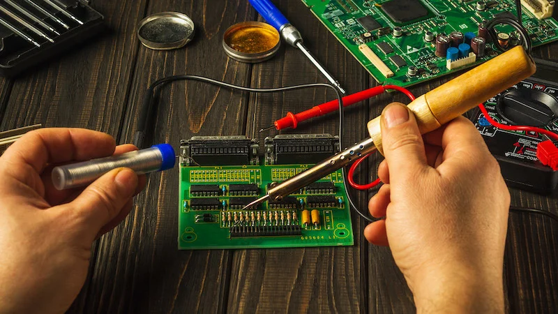
Image Source: EEpower.com
1.Gerber Files (RS-274X)
Gerber files are the super important ones in making PCBs. They hold all the design info for each layer, like copper paths, solder masks, silkscreen (the writing on parts), and where to drill holes. Manufacturers use these to build the actual PCB layers.
2.Drill Files (Excellon)
Drill files tell you where, how big, and what kind of holes to drill on the PCB. This includes vias, holes for component leads, and mounting spots. These are a must-have for drilling machines.
3.Netlist Files
Netlist files list all the electrical connections between parts. They help check if the PCB layout matches the design plan by verifying the connections.
4.Bill of Materials (BOM)
The BOM is a list of all the parts in the PCB, including their numbers, how many you need, and specs (like resistors, capacitors, and ICs). Procurement teams and manufacturers use it to buy and put together the parts.
5.Pick and Place Files (Centroid Files)
Pick and place files give the exact spot, direction, and reference name for surface-mount parts. Automated machines use these to place parts correctly on the board.
6.Schematic Files
Schematic files show the electrical design of the circuit, how parts are connected. It's the starting point for PCB layout and helps engineers picture the circuit.
7.Assembly Drawings
These files give detailed steps for putting the PCB together, like where to place parts, how layers stack up, and any special assembly rules. They help with both manual and automated assembly.
8.IPC-356 Files (Netlist Test Files)
IPC-356 files are for testing the PCB's electricity. They make sure the board has the right connections and no issues by providing test data for automated testers.
Why Is A BOM so Important for PCB Design
BOM (Bill of Materials) is extremely critical in PCB design because it is like a manual for finding parts, buying things, and assembling boards. Why is it so important? Listen to me tell you:
1.Complete list of parts
The BOM lists all the components used on the PCB, from resistors and capacitors to integrated circuits and connectors. Each component has its own unique number, description, and quantity, so that no one is missed during assembly.
2.Don't worry about buying things
With accurate part numbers and manufacturer information, BOM makes buying things super easy. The procurement team knows what to buy at a glance and won't waste time due to finding the wrong parts or parts out of stock.
3.Version Management Assistant
Design changes and revisions, but BOM can help you clarify which version used which parts. This way, manufacturers will not use the wrong parts or configurations, avoiding confusion between different versions of designs.
4.Quality control
A well crafted BOM can also help you control quality, as it specifies the specifications of the parts and the recognized manufacturers. In this way, the final product can ensure reliable performance.
How Do you Export PCB Design Files for Manufacturing
Here are the general steps for exporting PCB design files:

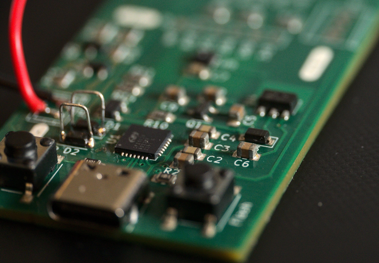
Image Source: BrixIT Blog.com
1.Prepare to export design
Before exporting, take a look at your PCB design to ensure it meets production requirements:
Do a Design Rule Check (DRC) and check in the design software for any violations such as line width or spacing.
Check the gaps, stacking structure, and via size of the board to ensure they match the manufacturer's requirements.
2.Export Gerber file
Gerber files are the most commonly used format for PCB manufacturing, containing detailed information about each layer of the PCB. Most PCB CAD tools have the option to generate Gerber files:
The layers to be exported must be complete, such as copper layer (top and bottom layers), solder mask layer, silk screen layer, and board outline.
The file format must use the standard RS-274X.
3.Export drilling files
Drilling files, usually in Excellon format, require clear hole diameters and positions for vias, through holes, and installation points
The drilling file must specify the diameter and X/Y coordinates of each hole.
Generate netlist (optional)
A netlist file is not necessary, but it can also be exported, listing the electrical connections between components. It can be of great use when comparing PCB layouts and schematics.
4.Create a Bill of Materials (BOM)
Export BOM, which should include:
Component identifier, part number, quantity, description (such as capacitance, resistance value).
BOM can help manufacturers find and assemble components correctly.
5.Export patch file (Centroid file)
SMT files are used for automated assembly and must indicate the precise coordinates, orientation, and type of SMT components:
The file format must be compatible with the manufacturer's SMT machine.
Export assembly drawing (optional)
If manual assembly or inspection is required, an assembly drawing may also need to be exported, indicating component positions, reference identifiers, and special instructions.
6.Package all files
After exporting the necessary files (Gerber, drilling, BOM, etc.), package them into a ZIP folder. Manufacturers generally prefer to collect compressed folders for better management.
7.Submit documents to the manufacturer
Once the files are ready, submit the ZIP folder to the PCB manufacturer, usually through their online portal or email. Don't forget to comply with any file format requirements that the manufacturer may have.
The Key Layers in A PCB Design
Speaking of PCB (printed circuit board), it is composed of many layers, each layer playing a unique role in the functionality and manufacturing of the board. Let's talk about the common key layers in PCB design below:
Copper layer
Signal layer (top and bottom layers): This is the conductive layer where the circuit (wiring) is laid out. Single sided and double-sided PCBs often use top and bottom layers to connect components.
Inner layer: In multi-layer boards, there is an additional internal copper layer used for laying signals, power supplies, and ground wires.
Solder mask layer
The solder mask layer is a protective layer applied to copper traces to prevent short circuits and oxidation. It covers the area between the traces, but the solder pads and vias are exposed, making it easier to solder components. The most common solder mask is green, but there are also red, blue, black and other colors.
Silkscreen
The silk screen layer is used to print labels, reference identifiers, logos, and component outlines on the board. This layer helps us identify components during assembly and troubleshooting, usually both the top and bottom layers.
Drilling layer
The drilling layer indicates the positions of all holes on the PCB, including:
Via: a small hole that connects different copper layers.
Through hole: a large hole for inserting component pins or installing components.
The drilling data will indicate the aperture and position of the through-hole and through-hole components.
Power and ground layer
Power layer: a large copper area specifically designed for conducting electricity (such as VCC). It can reduce resistance and improve conductivity.
Ground layer: Similar to the power layer, the ground layer provides a large, low impedance path for the return current, which can reduce noise and improve signal quality.
Pad layer
The pad layer defines the position where component pins are soldered onto the PCB. It can be a surface mount pad for SMD (Surface Mount Components), or a through-hole pad for components with pins passing through the board.
Mechanical layer
This layer defines the physical dimensions of the PCB, such as board contours, openings, mounting holes, and other mechanical features. Ensure that the PCB can be correctly installed into the casing or installation system.
Keep Out Layer
The prohibited wiring layer indicates areas where components or wiring cannot be placed. Used to leave space for mechanical components or high-voltage areas, to prevent interference or short circuits.
Wiring layer (inner layer of multi-layer PCB)
In multi-layer PCBs, internal wiring layers are used to distribute signals between different layers. These layers can make the design more complex, with additional routing paths, and the top and bottom layers alone are not enough.
Final Verdict
Understanding what file type is used for PCB designs involved in PCB design is crucial for ensuring a smooth transition from concept to manufacturing.
Files like Gerber, drill, BOM, and pick-and-place guide the fabrication and assembly processes, ensuring accuracy and efficiency.
By familiarizing yourself with these essential files, you can streamline your PCB design workflow and avoid potential errors in production.

Disclaimer: The views and opinions expressed by individual authors or forum participants on this website do not represent the views and opinions of Chipsmall, nor do they represent Chipsmall's official policy.

share this blog to:

