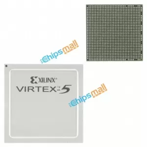

XC5VSX50T-2FFG665C
- Manufacturer's Part No.:XC5VSX50T-2FFG665C
- Manufacturer:
- Categories:
- Sub-Categories:
- Series:Virtex®-5 SXT
- Description:IC FPGA 360 I/O 665FCBGA
- Datasheet:
- Quantity:RFQAdd to RFQ List
- Payment:

- Delivery:

- Available: 10
Reference Price(In US Dollars)
| Qty | Unit Price | Ext.Price |
|---|---|---|
| 1+ | US $2.00000 | US $2.00 |
| 10+ | US $1.80000 | US $18.00 |
| 30+ | US $1.40000 | US $42.00 |
| 100+ | US $1.15000 | US $115.00 |
| 500+ | US $1.10000 | US $550.00 |
| 1000+ | US $1.00000 | US $1000.00 |
Do you want a lower wholesale price? Please send us an inquiry, and we will respond immediately.
- Description
- Alternatives
- Shopping Guide
The Motorola DSP56307, a member of the DSP56300 family of programmable digital signal processors (DSPs), supports wireless infrastructure applications with general filtering operations.
The on-chip enhanced filter coprocessor (EFCOP) processes filter algorithms in parallel with core operation, thus increasing overall DSP performance and efficiency. Like the other family members, the DSP56307 uses a high-performance, single-clock-cycle-per-instruction engine (code-compatible with Motorolas popular DSP56000 core family), a barrel shifter, 24-bit addressing, an instruction cache, and a direct memory access controller, as in Figure 1.
The DSP56307 offers performance at 100 million instructions (MIPS) per second using an internal 100 MHz clock with a 2.5 volt core and independent 3.3 volt input/output power.
FEATURESHigh-Performance DSP56300 Core● 100 million instructions per second (MIPS) with a 100 MHz clock at 2.5 V core and 3.3 V I/O● Object code compatible with the DSP56000 core● Highly parallel instruction set● Data arithmetic logic unit (ALU) - Fully pipelined 24 x 24-bit parallel multiplier-accumulator - 56-bit parallel barrel shifter (fast shift and normalization; bit stream generation and parsing) - Conditional ALU instructions - 24-bit or 16-bit arithmetic support under software control● Program control unit (PCU) - Position independent code (PIC) support - Addressing modes optimized for DSP applications (including immediate offsets) - On-chip instruction cache controller - On-chip memory-expandable hardware stack - Nested hardware DO loops - Fast auto-return interrupts● Direct memory access (DMA) - Six DMA channels supporting internal and external accesses - One-, two-, and three- dimensional transfers (including circular buffering) - End-of-block-transfer interrupts - Triggering from interrupt lines and all peripherals● Phase-locked loop (PLL) - Allows change of low power divide factor (DF) without loss of lock - Output clock with skew elimination● Hardware debugging support - On-Chip Emulation (OnCE) module - Joint test action group (JTAG) test access port (TAP) - Address trace mode reflects internal Program RAM accesses at the external port
Functional Equivalent (FE) materials, including Fused Filament Fabrication (FFF) form, assembly, and functionally compatible substitute materials.
SHIPPING GUIDE
Shipping Methods

Rest assured that your orders will be handled by these trusted providers, such as DHL, FedEx, SF, and UPS.
Shipping Cost

Shipping starts at $40 but varies for destinations like South Africa, Brazil, India, and more. The actual shipping charges depend on time zone, country, and package weight/volume.
Delivery Time

We ship orders once daily, around 5 p.m., except on Sundays. The estimated delivery time may vary depending on the courier service you choose, but typically ranges from 5 to 7 business days.
RELEVANT BLOGS & POSTS

Professional Platform

Full-speed Delivery

Wide Variety of Products

365 Days of Quality Assurance


