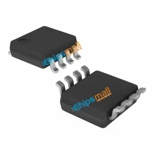

CLVC2G126MDCUTEP
- Manufacturer's Part No.:CLVC2G126MDCUTEP
- Manufacturer:
- Categories:
- Sub-Categories:
- Series:74LVC
- Description:IC BUFFER NON-INVERT 5.5V US8
- Quantity:Buy NowAdd to Cart
- Payment:

- Delivery:

- In Stock: 4775
- Available: 250
Reference Price(In US Dollars)
| Qty | Unit Price | Ext.Price |
|---|---|---|
| 1+ | US $34.68000 | US $34.68 |
| 10+ | US $26.01000 | US $260.10 |
| 30+ | US $22.54200 | US $676.26 |
| 100+ | US $19.94100 | US $1994.10 |
| 500+ | US $18.72720 | US $9363.60 |
| 1000+ | US $17.34000 | US $17340.00 |
Do you want a lower wholesale price? Please send us an inquiry, and we will respond immediately.
- Description
- Alternatives
- Shopping Guide
The CLVC2G126MDCUTEP is a dual non-inverting buffer/line driver IC designed for general-purpose logic level translation applications. It features two independent channels, each capable of driving a signal from a lower voltage (LV) to a higher voltage (HV), or vice versa, while providing high-speed performance and low power consumption.
Key Features:
- Dual Independent Channels: The IC consists of two identical buffer/line driver channels, allowing for simultaneous translation of two separate input signals to corresponding output signals.
- Non-Inverting Logic Translation: It provides non-inverting logic level translation, meaning that the output signal follows the logic state of the input signal without inversion.
- Wide Voltage Range: The CLVC2G126MDCUTEP supports a wide range of input and output voltage levels, making it suitable for interfacing between different logic families or voltage domains.
- High-Speed Operation: With fast propagation delays and transition times, the IC enables high-speed signal transmission, making it suitable for use in applications requiring rapid data transfer.
- Low Power Consumption: It is designed for low power consumption, helping to minimize energy usage and extend battery life in portable electronic devices.
- Latch-Up Performance: The IC exhibits excellent latch-up performance, ensuring robust operation and reliability in noisy or harsh electrical environments.
- ESD Protection: It incorporates electrostatic discharge (ESD) protection features to safeguard the device against damage from static electricity during handling and operation.
- Space-Saving Package: Housed in a compact leadless package (DCU), the CLVC2G126MDCUTEP offers space-saving advantages and facilitates high-density board layouts in space-constrained applications.
Applications:
- Level shifting and voltage translation in mixed-voltage systems
- Interface between different logic families (e.g., CMOS, TTL, LVCMOS)
- Signal buffering and line driving in data communication systems
- General-purpose digital signal level conversion
- Portable and battery-powered devices requiring low power consumption
Functional Equivalent (FE) materials, including Fused Filament Fabrication (FFF) form, assembly, and functionally compatible substitute materials.
SHIPPING GUIDE
Shipping Methods

Rest assured that your orders will be handled by these trusted providers, such as DHL, FedEx, SF, and UPS.
Shipping Cost

Shipping starts at $40 but varies for destinations like South Africa, Brazil, India, and more. The actual shipping charges depend on time zone, country, and package weight/volume.
Delivery Time

We ship orders once daily, around 5 p.m., except on Sundays. The estimated delivery time may vary depending on the courier service you choose, but typically ranges from 5 to 7 business days.
RELEVANT BLOGS & POSTS

Professional Platform

Full-speed Delivery

Wide Variety of Products

365 Days of Quality Assurance


